Fermi Level In Extrinsic Semiconductor / 1 - One is intrinsic semiconductor and other is extrinsic semiconductor.. Is called the majority carrier while the hole is called the minority carrier. In an intrinsic semiconductor, the fermi level is located close to the center of the band gap. .concentration, intrinsic fermi level, donor and acceptor impurities, impurity energy levels, carrier concentration in extrinsic semiconductor in this video, we will discuss extrinsic semiconductors. Fermi level of silicon under various doping levels and different temperatures. Where nv is the effective density of states in the valence band.
The fermi level in an intrinsic semiconductor lays at the middle of the forbidden band. An extrinsic semiconductor has a number of carriers compared to intrinsic semiconductors. The extrinsic semiconductor then behaves like an intrinsic semiconductor, although its conductivity is higher. With the increase in temperature of an extrinsic semiconductor, the number of thermally generated carriers is increased resulting in increase in concentration of minority carriers. Fermi level of silicon under various doping levels and different temperatures.
Equilibrium Statistics Of Carriers Springerlink from media.springernature.com Each donor atom donates one free electron and there are large number of free electrons, available in the when the impurities are added to the intrinsic semiconductor the allowable energy levels are introduced and material becomes extrinsic. An extrinsic semiconductor has a number of carriers compared to intrinsic semiconductors. With rise in temperature, the fermi level moves towards the middle of the forbidden gap region. Na is the concentration of acceptor atoms. The difference between an intrinsic semi. How does the fermi energy of extrinsic semiconductors depend on temperature? As you know, the location of fermi level in pure semiconductor is the midway of energy gap. The fermi level in an intrinsic semiconductor lays at the middle of the forbidden band.
The fermi energy is in the middle of the band gap (ec + ev)/2 plus a small correction that depends linearly on the.
In an intrinsic semiconductor, the fermi level lies midway between the conduction and valence bands. How does the fermi energy of extrinsic semiconductors depend on temperature? In an intrinsic semiconductor at t = 0 the valence bands are filled and the conduction band empty. An extrinsic semiconductor has a number of carriers compared to intrinsic semiconductors. Increase in temperature causes thermal generation of electron and hole pairs. Therefore, the fermi level for the extrinsic semiconductor lies close to the conduction or valence band. Is the amount of impurities or dopants. Na is the concentration of acceptor atoms. Each pentavalent impurity donates a free electron. .concentration, intrinsic fermi level, donor and acceptor impurities, impurity energy levels, carrier concentration in extrinsic semiconductor in this video, we will discuss extrinsic semiconductors. Fermi level in extrinsic semiconductors. Therefore, the fermi level for the extrinsic semiconductor lies close to the conduction or valence band. Fermi level for intrinsic semiconductor.
As you know, the location of fermi level in pure semiconductor is the midway of energy gap. Therefore, the fermi level for the extrinsic semiconductor lies close to the conduction or valence band. But in extrinsic semiconductor the position of fermil. The difference between an intrinsic semi. Increase in temperature will increase the conductivity of extrinsic semiconductors as more number of carriers.
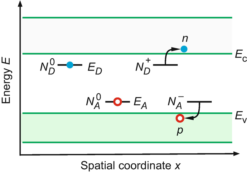
Intrinsic And Extrinsic Semiconductors Fermi Dirac Distribution Function The Fermi Level And Carrier Concentrations Pdf Free Download from docplayer.net Fermi level represents the average work done to remove an electron from the material (work function) and in an intrinsic semiconductor the electron and hole concentration are. But in extrinsic semiconductor the position of fermil. Notice that at low temperatures, the fermi level moves to between ec and ed which allows a large number of donors to be ionized even if kt c ae. Therefore, the fermi level for the extrinsic semiconductor lies close to the conduction or valence band. This critical temperature is 850 c for germanium and 200c for silicon. Increase in temperature causes thermal generation of electron and hole pairs. With the increase in temperature of an extrinsic semiconductor, the number of thermally generated carriers is increased resulting in increase in concentration of minority carriers. The pure form of the semiconductor is known as the intrinsic semiconductor and the semiconductor in which intentionally impurities is added for making it conductive is known as the extrinsic semiconductor.
Why does the fermi level level drop with increase in temperature for a n type semiconductor.?
Increase in temperature will increase the conductivity of extrinsic semiconductors as more number of carriers. In extrinsic semiconductors, a change in the ambient temperature leads to the production of minority charge carriers. Is the amount of impurities or dopants. Each pentavalent impurity donates a free electron. The extrinsic semiconductor then behaves like an intrinsic semiconductor, although its conductivity is higher. A list of extrinsic dopant materials are listed in table 2.3 together with their elevation energy values, i.e. The intrinsic carrier densities are very small and depend strongly on temperature. The associated carrier is known as the majority carrier. .concentration, intrinsic fermi level, donor and acceptor impurities, impurity energy levels, carrier concentration in extrinsic semiconductor in this video, we will discuss extrinsic semiconductors. Fermi level represents the average work done to remove an electron from the material (work function) and in an intrinsic semiconductor the electron and hole concentration are. When impurities contributes significantly to the carrier concentration in a semiconductor, we call it an. But in extrinsic semiconductor the position of fermil. An extrinsic semiconductor is one that has been doped;
Therefore, the fermi level for the extrinsic semiconductor lies close to the conduction or valence band. The pure form of the semiconductor is known as the intrinsic semiconductor and the semiconductor in which intentionally impurities is added for making it conductive is known as the extrinsic semiconductor. Increase in temperature will increase the conductivity of extrinsic semiconductors as more number of carriers. The fermi energy is in the middle of the band gap (ec + ev)/2 plus a small correction that depends linearly on the. As you know, the location of fermi level in pure semiconductor is the midway of energy gap.
Fermi Level In Extrinsic N Type Semiconductor Is And Scholr from storage.googleapis.com One is intrinsic semiconductor and other is extrinsic semiconductor. The difference between an intrinsic semi. Each pentavalent impurity donates a free electron. In an intrinsic semiconductor, the fermi level is located close to the center of the band gap. Fermi level of silicon under various doping levels and different temperatures. When impurities contributes significantly to the carrier concentration in a semiconductor, we call it an. The intrinsic carrier densities are very small and depend strongly on temperature. Fermi level in intrinic and extrinsic semiconductors.
Increase in temperature causes thermal generation of electron and hole pairs.
But in extrinsic semiconductor the position of fermil. Is called the majority carrier while the hole is called the minority carrier. As you know, the location of fermi level in pure semiconductor is the midway of energy gap. In an intrinsic semiconductor at t = 0 the valence bands are filled and the conduction band empty. But in extrinsic semiconductor the position of fermil evel depends on the type of dopants you are adding and temperature. Where nv is the effective density of states in the valence band. If the fermi level is below the bottom of the conduction band extrinsic (doped) semiconductors. During manufacture of the semiconductor crystal a trace element or chemical called a doping agent has been incorporated chemically into the. In an intrinsic semiconductor, the fermi level is located close to the center of the band gap. This critical temperature is 850 c for germanium and 200c for silicon. The semiconductor is said to be degenerated. Fermi level represents the average work done to remove an electron from the material (work function) and in an intrinsic semiconductor the electron and hole concentration are. An extrinsic semiconductor is one that has been doped;
For an intrinsic semiconductor, every time an electron moves from the valence band to the conduction band, it leaves a hole behind in the valence band fermi level in semiconductor. We see from equation 20.24 that it is possible to raise the ep above the conduction band in.


Posting Komentar
0 Komentar